
From Lasers to Lab-on-a-Chip: How Integrated Photonics Is Quietly Rewiring Technology

Multi-beam, laser Doppler vibrometer for medical use, using silicon photonics in a glass-based package developed in PhotonicLEAP project. Credit: PhotonicLEAP.
If you took apart your smartphone, you would find astonishing layers of electronic sophistication. But what you would not obviously see (yet) is light.
That, says Dr. Sylwester Latkowski of Eindhoven University of Technology and Scientific Director of the Photonic Integration Technology Center (PITC), is about to change.
“I want people to know that there is a photonic integrated circuit (PIC) in their smartphone,” he told me after his lecture. “Some smartphones have them already in a simple form, but still not enough.”
Latkowski works in integrated photonics: the art of building semiconductor chips that manipulate light instead of, or alongside, electricity. These chips can generate laser light, guide it through microscopic waveguides thinner than a human hair, modulate it, detect it and process information at extraordinary speeds and with exceptional energy efficiency.
In his lecture, part of the QAMSS lecture series held at the at the Cambridge Graphene Centre (CGC), titled Integrated Photonics Technologies, he showed how this technology is moving far beyond its traditional home in telecommunications. Photonic chips are now central to sensing, medical devices, quantum technologies, AI hardware and even environmental monitoring. But his talk was not just about devices. It was about something more ambitious: turning photonics into a mature, standardised industrial technology, on par with microelectronics.
That is a surprisingly hard problem.
A system on a chip, but for light
Modern integrated photonics is, in Latkowski’s words, a “system on a chip.” Instead of assembling bulky optical setups with mirrors and lenses, engineers can now integrate lasers, modulators, amplifiers, filters and detectors onto a single millimetre-scale semiconductor die.
Many of these chips are built using indium phosphide (InP), a material that can naturally generate laser light. At TU Eindhoven, Latkowski’s group has an 800 m² cleanroom (Figure 1) dedicated to fabricating such chips, capable of full wafer-scale processing.
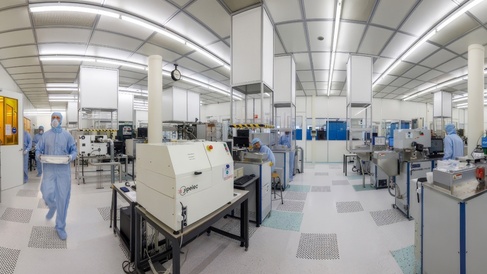
Figure 1: InP chip fabrication. Credit: NanoLab@TU/e.
But building a photonic chip is only half the battle.
“Integrated photonics can be tiny and demanding,” he said during the lecture. “Optical alignment is challenging. Optical probing is challenging. There are no standard interfaces. No standard tools for test, assembly and packaging.”
Electronics solved these problems decades ago. Photonics hasn’t, yet.
That gap is where much of Latkowski’s work now sits, making photonic chips not just impressive research demonstrations, but reliable, testable manufacturable products.
The laser that can smell
One of the most striking examples he presented was a photonic chip designed for gas sensing.
Certain gases absorb light at extremely precise wavelengths. If you can build a laser that can tune with exquisite precision across those wavelengths, you can detect gases like acetylene, ammonia, hydrogen cyanide and even carbon dioxide simply by measuring how much light is absorbed.
This requires lasers that are astonishingly well behaved: linewidths of only a few hundred kilohertz, tuning ranges of tens of nanometres, and stability down to picometres in wavelength.
Latkowski’s group demonstrated a chip containing four independently tunable lasers, integrated together with on-chip wavelength monitoring. These lasers can sweep across absorption lines and detect gas signatures with extraordinary sensitivity.
And then they asked a provocative question: what if we did this not only at the standard telecom wavelength of 1.55 µm, but also at 2 µm, where many more gases have strong absorption features?
That required rethinking the entire waveguide and amplifier design, because materials that work beautifully at 1.55 µm become lossy at 2 µm. The result was the first long-wavelength multi-project wafer run in their foundry, an important step toward opening entirely new application domains.
This is not just about industrial gas sensing. It could enable environmental monitoring, breath analysis for medical diagnostics and portable sensing devices.
Latkowski sees a trajectory here.
“First it’s a toy,” he said with a smile, “and then eventually we try to make it a medical device.”
From cameras to pills
That comment was not hypothetical. In the interview, he described an idea he once explored with colleagues: combining photonics with ingestible medical devices.
There are already swallowable “camera pills” that image the digestive tract. Latkowski’s thought was to add optical coherence tomography, a photonic imaging technique that can see microscopic structure beneath the surface.
“We put PIC inside, and we can do optical coherence tomography at the same time images are being taken,” he explained. “It would really enhance diagnostic capabilities.”
The idea was never fully pursued, but it illustrates how integrated photonics naturally lends itself to miniaturised, highly functional sensing in places traditional optics cannot reach.
Why AI is suddenly interested in photonics
In recent years, AI hardware has become a surprising driver for photonics.
Training large AI models requires immense data transfer and power consumption. Companies like Intel and Nvidia have publicly announced that their AI supporting products will feature photonic chiplets to move data using light instead of electricity inside computing systems.
Latkowski sees this as a turning point.
“When the giants of the semiconductor microelectronics sent a message, ‘We need a photonic chiplet,’ all eyes [turned] on us,” he said. “It’s a blessing for us.”
At the same time, AI may help photonics, and even the semiconductor industry, solve one of its internal problems: manufacturing complexity. Fabrication processes generate vast amounts of data, and while AI can greatly help in interpreting this, and even making decisions, companies are cautious about using cloud-based AI because of data security concerns.
“The information can easily leave premises,” he said, describing manufacturers’ fears. But he believes edge-based AI and specialised AI tools will eventually allow process optimisation without compromising confidentiality.
The real bottleneck: Packaging and testing
Perhaps a surprising part of Latkowski’s lecture was the focus on testing, packaging and standardisation.
He showed elaborate glass interposers with through-glass vias, ball grid arrays, automated probing systems with over a thousand electrical contacts, and software frameworks to describe photonic packages in standardised data formats.
Why?
Because, as he put it, without this infrastructure, photonics will remain a niche research technology.
“The designer of the PIC is typically a photonics expert, someone with a PhD,” he said. “The electronic IC… can be designed by high school students. That shows how mature the field is.”
Photonics must reach that level of maturity. That requires process design kits (PDKs), design rules, interoperable software tools and standard packaging approaches so that engineers from different disciplines can work together without speaking different “languages”.
“It has to be interdisciplinary now,” he said. “Otherwise, the design team will be too large… humans make errors.”
From debate to progress
Latkowski’s approach to research is shaped by an enthusiasm for disagreement.
He recounted choosing as his PhD examiner, Prof. Erwin Bente, a scientist known to question Latkowski’s work. “Erwin loves to work with people that he disagrees with,” he said. “Because then we can have a debate.”
Shortly after the PhD viva, they become fellow researchers, and are colleagues in the same group at TU/e. He brings the same philosophy to his team.
“If they all agree I’m saying something is wrong. The best ideas and progress come from debate.”
That openness is perhaps essential in a field that sits at the crossroads of materials science, electronics, optics, software and mechanical engineering.
Where this is going
So where does he see integrated photonics heading?
“More and more intimate integration with microelectronics and different materials,” he said. “More wavelength bands within a single chip… technology will be a fusion of multiple technologies.”
Instead of one photonic platform trying to do everything, future chips will combine materials optimised for different tasks, bonded together into hybrid systems.
The ultimate goal is that photonics becomes invisible in the best possible way: embedded everywhere, enabling faster communication, better sensing and more sustainable technology.
“We can make access to information better, faster, maybe more energy efficient,” he said. “That’s what photonics enables.”
And perhaps, one day, that tiny chip manipulating light will sit quietly inside your phone, your medical device or a sensor you didn’t even know was there, doing work that once required an entire optical laboratory.
Just as electronics did half a century ago, photonics is preparing to disappear into everyday life.
About the interviewee

Sylwester Latkowski obtained MSc and Eng degrees in optoelectronics and technical physics from the West Pomeranian University of Technology in Szczecin, Poland, and a PhD in photonics at the Centre for High-Speed Devices and Systems at Dublin City University, Ireland. His early research concerned mode-locked semiconductor lasers, millimeter and terahertz photonics and all-optical signal processing for data transmission in optical networks. Sylwester followed up his interests with the Photonic Integration group at Eindhoven University of Technology (TU/e), the Netherlands, focusing on test assembly and packaging of integrated photonics, photonic integration technologies and on-chip laser systems for sensing applications. He is also scientific director at the Photonic Integration Technology Center (PITC) where he is responsible for shaping the strategic R&D agenda of shared research program lines and engagement with industry.
A chair and co-chair of the electronic-photonic test Technical Working Group of the Integrated Photonic Systems Roadmap International, Sylwester also represents PITC in the steering committee of the joint European platform for photonic integrated components and circuits, JePPIX. He is a senior member of the IEEE and IEEE Photonics Society and a voting member of the IEEE Standards Association and Photonic Standards Committee. Sylwester chairs the working group for the standardization of electronic-photonic design automation, IEEE SA P3112 and serves as a Senior Editor for the IEEE Photonics Journal.
He has authored and co-authored more than 135 publications in international scientific journals and conference proceedings.
By Dr Karen Steward